


韩国 8 英寸纯晶圆代工厂 SK keyfoundry 近日宣布推出用于电容器的多层厚 IMD(金属间电介质)工艺,该工艺具有业界领先的高击穿电压特性。
SK Keyfoundry, an 8-inch pure-play foundry in Korea, has recently announced the launch of its Multi-Layer Thick IMD (Inter-Metal Dielectric) process for capacitors, which boasts industry-leading high breakdown voltage characteristics.
数字绝缘体的高击穿电压特性增强了半导体器件的安全性和可靠性,并提高了其使用寿命和抗噪能力。全新的多层厚IMD工艺能够堆叠多达三层金属间介电层 (IMD),每层最大厚度为6μm,在金属-绝缘体-金属 (MIM) 结构中形成总厚度高达18μm的IMD。这不仅提供了高达19,000V的高击穿电压特性,还具有高电容性能。该工艺预计将用于制造用于数字隔离和抑制电子电路电容耦合的电容器。
High breakdown voltage characteristics of digital insulators enhance the safety and reliability of semiconductor devices, and also improve their lifespan and noise immunity. The new Multi-Level Thick IMD process enables the stacking of up to three inter-metal dielectric (IMD) layers, each with a maximum thickness of 6μm, creating a total thickness of up to 18μm in a metal-insulator-metal (MIM) structure. This provides high breakdown voltage characteristics of up to 19,000V along with high capacitance performance. The process is expected to be used in the manufacturing of capacitors for digital isolation and for suppressing capacitive coupling in electronic circuits.
采用该工艺生产的电容器已成功通过主要客户的TDDB(时间相关介质击穿)评估,并符合AEC-Q100国际汽车半导体质量标准,可在恶劣环境下实现高可靠性运行。尤其值得一提的是,该工艺可集成到0.13µm和0.18µm BCD工艺技术中,使其在汽车半导体领域具有极强的适用性。此外,该工艺还提供PDK(工艺设计套件)、DRC、LPE、LVS和Pcell等设计支持工具,帮助客户加速产品开发。
Capacitors manufactured with this process have successfully passed major customers’ TDDB (Time Dependent Dielectric Breakdown) evaluations and have met the AEC-Q100 international automotive semiconductor quality standard for high-reliability operation in harsh environments. In particular, the process can be integrated into 0.13µm and 0.18µm BCD process technologies, making it highly applicable to the automotive semiconductor field. In addition, design support tools, including PDK (Process Design Kit), DRC, LPE, LVS, and Pcell, are provided to help customers accelerate product development.
SK keyfoundry 强调,与基于传统光隔离器的设备相比,这种数字隔离技术将为电动汽车、工业、电信和医疗保健领域中需要高抗噪能力的电子设备在性能、可靠性、集成度和成本效益方面提供竞争优势。
SK keyfoundry highlighted that this digital isolation technology will offer a competitive advantage in performance, reliability, integration, and cost-efficiency for electronic devices that require high noise immunity in the fields of EVs, industry, telecommunications, and healthcare, compared to devices based on conventional optical isolators.
SK keyfoundry 首席执行官 Derek D. Lee 表示:“我们很高兴推出业界领先的数字绝缘体多层厚 IMD 工艺技术,该技术正受到包括电动汽车在内的整个电子行业的关注。SK keyfoundry 将利用我们相比竞争对手更出色的量产经验,不仅为国内客户,还为美国、中国等海外客户提供世界一流的工艺技术,持续开发满足多样化客户需求的高可靠性隔离技术。”
“We are pleased to introduce our industry-leading Multi-Level Thick IMD process technology for digital insulators, which is gaining attention across the electronics industry, including EVs,” said Derek D. Lee, CEO of SK keyfoundry. “SK keyfoundry will continue to develop highly reliable isolation technologies that meet diverse customer needs by providing world-class process technologies not only to domestic customers but also to overseas customers, including in the United States and China, leveraging our outstanding mass production experience compared to competitors.”
多层厚 IMD(金属间电介质)工艺介绍
Introduction to Multi-Layer Thick IMD (Inter-Metal Dielectric) Process
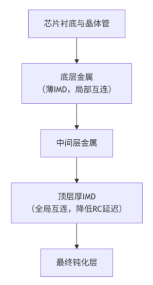
多层厚金属间电介质工艺是一种用于先进半导体制造的关键技术,它指在芯片后道工艺中,于上层较宽的全局互连金属线之间,沉积显著增厚的绝缘介质层;这种“厚IMD”结构能有效降低金属线间的寄生电容,从而减少信号传输延迟和功耗,提升芯片整体性能。
The multi-layer thick metal inter-dielectric process is a key technology used in advanced semiconductor manufacturing. It refers to the deposition of significantly thick insulating dielectric layers between wider global interconnect metal lines in the backend of chip processing. This 'thick IMD' structure can effectively reduce the parasitic capacitance between metal lines, thereby reducing signal transmission delay and power consumption, and improving the overall performance of the chip.
关于SK keyfoundry
About SK keyfoundry
SK keyfoundry 总部位于韩国,为半导体公司提供专业的模拟和混合信号代工服务,服务于消费电子、通信、计算、汽车和工业领域的广泛应用。凭借广泛的技术组合和工艺节点,SK keyfoundry 拥有灵活性和能力,能够满足全球半导体公司不断变化的需求。
Headquartered in Korea, SK keyfoundry provides specialty Analog and Mixed-Signal foundry services for semiconductor companies to serve a wide range of applications in the consumer, communications, computing, automotive and industrial industries. With a broad range of technology portfolios and process nodes, SK keyfoundry has the flexibility and capability to meet the ever-evolving needs of semiconductor companies across the globe.
内容来源:SK keyfoundry官网;网址:https://www.skkeyfoundry.com/cn/ir/ir_sub02_view.html?seq=333&page=1。
Source of content: SK keyfoundry official website;Website: https://www.skkeyfoundry.com/cn/ir/ir_sub02_view.html?seq=333&page=1.
长按识别二维码关注公众号,点击下方菜单栏左侧“微信群”,申请加入交流群。
